

Innovative Approach to Transistor Creation Using Tungsten Ditelluride Monolayer
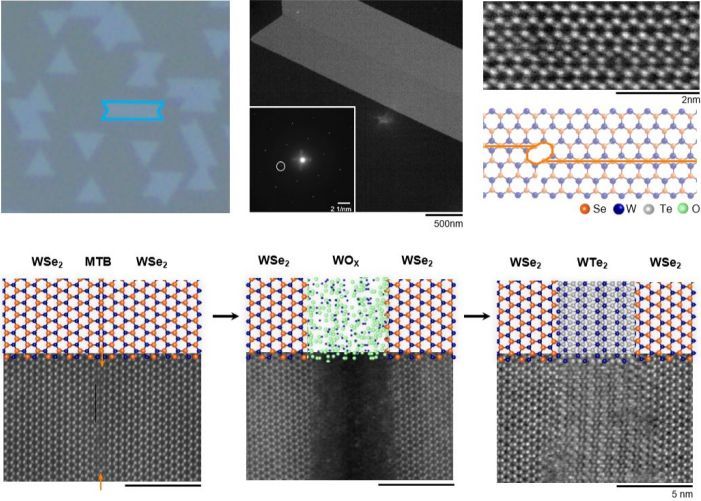
Researchers have recently reported a novel method for creating transistors directly within a tungsten ditelluride (WTe2) monolayer, which could significantly advance semiconductor technology. This approach eliminates the need for multiple rounds of modifications typically required in silicon semiconductor processes.
The study, led by Seok Young Min and colleagues, focuses on the in-situ creation of transistors by selectively transforming parts of the top layer into tungsten oxide (WOx) for insulation and other sections into n-type WS2 and p-type WSe2. This method allows for the construction of functional MOSFETs without the usual grafting of different materials.
One of the main advantages of this technique is its ability to operate at an atomic scale, potentially achieving higher density structures compared to conventional silicon semiconductor technologies. This advancement could pave the way for more compact and efficient electronic devices.
While WTe2 is a promising candidate, other transition-metal dichalcogenides (TMDCs) are also being explored for similar applications. For instance, research from 2014 by N. Lu et al. investigated the use of MoSe2 for creating two-dimensional semiconductors, which refers to the thin layers of these monolayer TMDCs.
As the field of two-dimensional materials continues to evolve, the findings from this research may lead to significant breakthroughs in the development of next-generation semiconductor devices.
Source: Hackaday